 LOGIN
LOGIN REGISTER
.png)


Research article
Design of a Plasmonic Refractive Index Sensor Based on the Amplifier System with Two Plasmonic Waveguides and Four Cavities with Different Dimensions and Coordinates
Hamid Abbasi
Atomic and molecular of Physics group, faculty of basic science, University of Mazandaran, Babolsar, Iran
*Corresponding author: HamidAbbasi, Atomic and molecular of Physics group, faculty of basic science, University of Mazandaran, Babolsar, Iran, Email: abbasiamolihamid6@gmail.com
Received Date: 04 July, 2023; Accepted Date: 20 July, 2023, Published Date: 28 July, 2023
Abstract
In this research, we design a plasmonic refractive index sensor based on metal insulated metal waveguide (MIM) and examine it numerically. To design the structure of this sensor, we use five cavities with different dimensions and coordinates and two plasmonic waveguides. The resonant wavelengths and refractive index of the resonators are investigated and simulated by the finite difference time domain (FDTD) method. Due to the fact that the sensors and conduction characteristics of plasmonic waves are affected by the structure parameters, by changing the refractive index and changing the dimensions of the cavities, we can weaken or strengthen the passage coefficient in the resonant modes. As a result, we obtain the sensitivity coefficient, the competency digit (FOM) and the sensor quality coefficient. These plasmonic sensors with a simple frame and high optical resolution can be used to measure the refractive index in the medical, chemical and food industries, and due to the special correct distribution of resonances, they are highly sensitive to changes in the refractive index of the environment.
Keywords: Plasmonics; Surface plasmon polaritons; Metal-Insulator-Metal; Refractive index sensor
Introduction
Optical integrated circuits are one of the most important and practical tools in technology. To further exploit them and reduce barriers, compression of plasmonic structures began. These structures are made of metal and dielectric with dimensions below the excitation wavelength. Plasmonic science expresses the interaction of radiant electromagnetic waves on the surface of metals and their conducting electrons and has the ability to enclose electromagnetic waves at dimensions much smaller than the radiant wavelength in plasmonic structures. The term plasmon polariton is used to describe the cause of this married condition. Plasmonics are divided into two parts: (1) localized surface plasmons and (2) surface polariton plasmons, each of which is an application of metals and electromagnetic waves (in nanometer dimensions) in two-dimensional and one-dimensional structures. . In localized surface plasmons (1), the oscillations of metal electrons and the intensification of plasmons are stimulated by the radiation beam, and the condition of the oscillation is that the frequency of the surface electrons is equal to the frequency of the radiation beam. The interaction of electromagnetic waves with excitation wavelength λ with a particle of size d can be studied in various numerical, analytical and semi-analytical methods. In this nano-volume, the electromagnetic field is compressed and modified. Also, small changes in the dielectric of this nanoparticle change the surface plasmon intensification, wavelength, absorbed and scattered beam, and the amount of these changes can be obtained by using optical characteristics. Plasmon Surface polaritons are electromagnetic waves that are coupled to surface free electrons in metals so that they can propagate longitudinally across the dielectric metal surface and have longitudinal polarization (P- polarized). One of the important applications of surface plasmon is to reduce the scattering of the electromagnetic field in optical waves and to confine the emission modes of the transverse electric field or the transverse magnetic field in the planes perpendicular to the direction of propagation. Surface plasmon amplification is an electromagnetic mode in which an electric field with TM polarization at the boundary between a metal surface and a dielectric material oscillates with paired electrons and two waves intensively occur, which increases the field strength. Electrical and sensor performance correction. Plasmonic structures are divided into metal-dielectricmetal and dielectric-metal-dielectric structures to study the propagation of waves. The most important plasmonic components are based on the structure of passive devices (such as waveguides, couplers, filters, etc.) and active devices (such as amplifiers, amplifiers, switches, modulators, etc.) and will be simulated numerically. Inactive environments are isotropic and have only one refractive index. As a result, they are unsuitable for switches and sensors, but active environments are anisotropic, and we can change the refractive index and length by applying an external factor. Plasmonic nanosensor systems are key components of optical integrated circuits that need to be developed. Parameters such as high transmission efficiency, high resolution, high quality factor, optical stability, sensitivity enhancement and adjustability in a range of wavelengths should be considered in the structure of plasmon sensors. Obtaining and improving these parameters increases the speed of information processing in optically integrated circuits. In this research, arrays of metal- dielectric waveguides and plasmonic resonators (MIM) are simulated and analysed to, design and fabricate plasmonic sensors. The aim of this work is to achieve the desired parameters in plasmonic sensors and to improve and develop it. Is. Therefore, we change the geometry of the waveguides and resonators, the refractive index of the dielectric region, and the direction of coupling to achieve our goal. Plasmonic sensors are divided into three categories based on their geometric shape: (1) plasmonic converters in which flat Nano film is used, (2) nanosensors with periodic nanowires, and (3) nanosensors containing single nanoparticles. In this research, changing the refractive index of the rims and changing the distance of the rims is used to improve the performance and adjust the plasmonic sensor systems.
Structural model and theory analysis
Each waveguide with any geometric shape has the ability to transmit waves and can limit their energy in one and two dimensions. This transition is interpreted by the wave equation. The geometry of a waveguide indicates its function, and the frequency of the transmitted wave determines the size of a waveguide. Maxwell’s equations describe the shape of electromagnetic cross waves and the linear electricity equation describes the shape of sound waves. At longer wavelengths, wider wavelengths are guided, and at higher frequencies, narrower wavelengths are guided. Above a frequency range, the optical properties of metals are explained by the plasma model, which is the result of Maxwell’s equations, and the electrons will be damped by collisions with the frequency υ = 1 / τ. For visible frequencies (microwave and far infrared), the spectrum of metals is very reflective and does not allow electromagnetic waves to propagate through them. At higher frequencies (near-infrared and visible from the spectrum) the field penetration and dissipation increase.
Then, at ultraviolet frequencies, the metals acquire dielectric properties and allow the propagation of electromagnetic waves with different degrees of attenuation. In the free electron model at high frequencies, the dielectric function tends to zero, and for noble metals, generalizing this model to a frequency range greater than the plasma frequency creates a polar environment. As a result, real metals are expressed by the greeting model:
ε) ω (=ε∞ - ωp2 / ω2+ iϒω (1)
ω is the angular frequency, ð–¼∞ = 1 is the dielectric constant of infinite frequency, ωp = 1.37 × 10¹⁶ is the plasma frequency and γ = 3.21 × 10¹³ is the electron oscillation frequency. The Droud model provides a microscopic description of metal dynamics in the form of classical sentences. The proposed structure is shown in Figure 1, which consists of two waveguides and five cavities, one cavity in the middle of two waveguides, two cavities at a distance of 12 nm at the top and a cavity at a distance of 12 nm at the bottom of the middle cavity. A cavity is located on the left, at a distance of 10 nm from the waveguide. The input wave goes from the left waveguide to the cavities and after passing through them goes to the output waveguide. The height of the two waveguides is w1 = 50 nm. The middle cavity located in the middle of the two waveguides has alength of L1 = 262 nm and a height of W2 = 60 nm, which is located at a distance of 19 nm from the two waveguides. The lower cavity has a length of L2 = 100 nm and a height of W3 = 100 nm and the three upper cavities have a length of L3 = 100 nm, L4 = 100 nm and L5 = 30 nm and a height of W4 = 100 nm, W5, respectively. = 220 nm and W6 = 130 nm. Pin and Pout are the input wave and output wave measurement monitors, respectively, which are calculated by merging the natural component of the Point Ting vector along the blurred lines. The transfer is calculated by T = Pout / Pin (Figure 1).
We consider the simulation bed as silver and the environment inside the cavities and waveguides as air. An electromagnetic field is generated by the excitation of a sensing element using light generated by SP that is
concentrated on the metal surface. The refractive index of the MIM changes when the material under contact contacts the sensor. SPs are very sensitive to changes in refractive index in the vicinity of the surface. Refractive index changes can be related to SP by measuring changes in one of the properties of light (such as changes in λres, intensity, or phase). Because the wavelengths of the waveguides are smaller than the wavelengths of the light emitted, only the plasmonic TM state is present in the structure. According to Fig.1, the TM wave, which is used for SPP excited waves, starts propagating from the left waveguide and propagates in the waveguide, and its intensity decreases as it gets closer to the output port. Each amplifier reflects a certain amount of input wave. We see the distribution of the electric field in the resonant frequency of the simulated structure in Figure

Figure 1: Two-dimensional image of a plasmonic sensor.
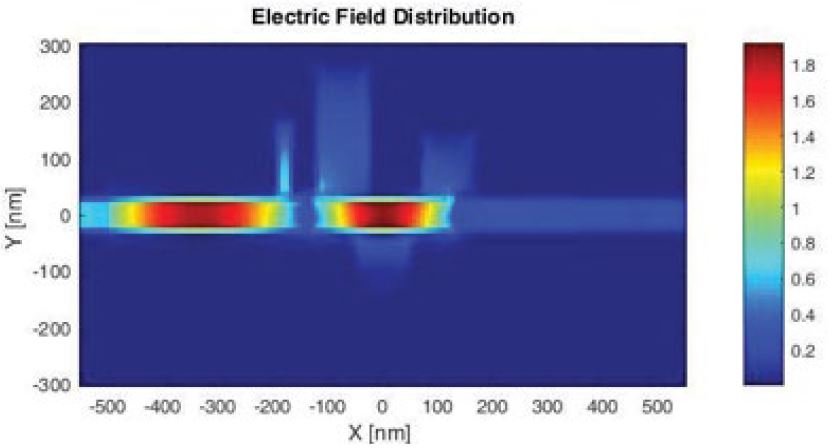
Figure 2: Electric field distribution at resonant frequency.
2, which according to the figure, the maximum radiation in the middle cavity. When the field distribution in cavities is similar, energy loss is reduced. To achieve the maximum field distribution in the structure, all dimensions must be optimal, otherwise we must change the dimensions of the structure to achieve the maximum field distribution (Figure 2).
Fracture coefficient simulation and measurement methods
The proposed plasmonic resonance behaviour is investigated numerically and theoretically. In the numerical approach to simulate the reflection spectrum and distribution of the optical field in the sensor structure, we use the time domain finite difference simulation (FDTD) method with perfectly matched layer boundary conditions (PML) because this method effectively reduces the numerical reflection. Gives. The uniform mesh sizes for the x and y directions are 8 and 8 nm, respectively, and the transmission line model is used to analyse the theory of structure. Twodimensional simulation is performed, which is infinite in one dimension. The reason for this is to reduce the simulation time and achieve the desired result. The effective refractive index of a four-cavity sensor with a step of 0.01 from 1 to 1.2 in the wavelength range of 400 to 1500 nm has been calculated, which leads to a change in spectra and resonance wavelength. (Figure 3) shows.
The first characteristic to be measured for a sensor is the S sensitivity, which is used to quantify the sensitivity of refractive index sensors:
S = Δ λ/ Δn (nm/RIU) (2)
In this equation, Δλ is the change in resonance wavelength and Δn is the change in refractive index. In this simulation, we only change the refractive index of the middle cavity, and the refractive index of the other cavities is constant, which will make the sensor design more accurate and practical. According to Figure 3, the sensor transmission spectra have two peaks, which according to Fig.4, have the highest sensitivity for the refractive index n = 1.19 (in mode2), which is equal to 1647 nm / RIU and the lowest value for the refractive index n = 1.18 (In mode1) is equal to 0 (Figure 4).
Using Fig.4, we analyse the refractive index and the amount of change in each wavelength to design our desired sensor. According to this diagram, there is a relatively linear relationship between the two parameters of resonance wavelength and refractive index, and the TM resonance gradually shifts. Therefore, using Equation 2, the sensitivity of different wavelengths is obtained. Let (Figure 5).
According to the figure, mode 2, which corresponds to the right peak of Fig.3, is more sensitive, and mode1, which

Figure 3: Transmission spectra of plasmonic refractive index sensor.

Figure 4: Resonance wavelength versus refractive index analysis.
corresponds to the left peak of Fig.3, has less sensitivity. Since sensitivity alone is not a measure of good performance for comparing different types of sensors, and light resolution is also very important for sensors, we need two more to measure the capabilities of a plasmonic sensor: Q quality factor and FOM suitability. Higher sensitivity reduces the FOM at the desired point. Obviously, increasing the length of the cavities can improve the sensitivity performance of the sensor with a smaller FOM size, which may result in a longer light path and more energy loss, respectively (Figure 6). The FOM merit is obtained from Equation (3):
FOM = S / FWHM (3)
Using Equation 3, we plot the FOM competency chart.
The quality coefficient is also obtained from Equation 4:
Q = λres / FWHM (4)
We see the quality coefficient diagram in (Figure 7)
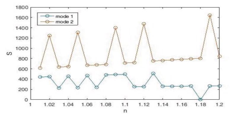
Figure 5: Plasmonic sensor sensitivity coefficient diagram.
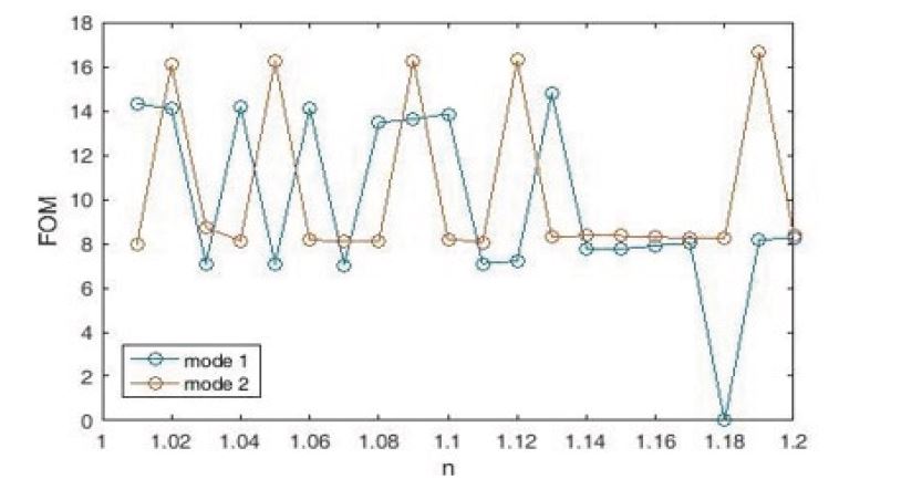
Figure 6: Plasmonic sensor FOM competency diagram.
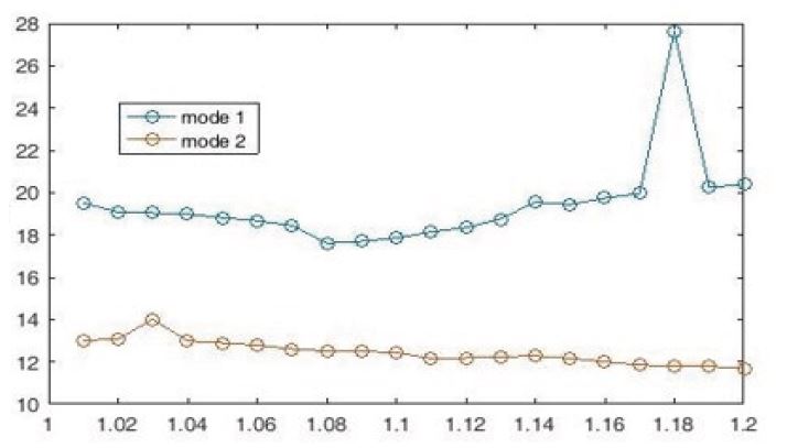
Figure 7: Quality factor diagram of Q plasmonic sensor.
Using Equation 4 and dividing the wavelength by FWHM, the quality coefficient Q is obtained and its value in the refractive index n = 1.19, which has the highest sensitivity coefficient, reaches 11.7935. Equations 2, 3 and 4 are the capabilities of measuring plasmon sensors obtained by changing the refractive index in the structure. Using these three equations, we draw the graphs of sensitivity coefficient, quality coefficient and competence. The remarkable thing about the proposed method is that its sensitivity coefficient is higher compared to previous sensors. As shown in Table 1, the proposed method offers better results compared to some similar articles. According to this table, the maximum sensitivity coefficient S among these papers belongs to the structure studied in this paper, which is equal to 1647 nm (Table 1).
Conclusion
Plasmonic refractive index sensor is a widespread issue and has become very popular in chemical and biological measurements because of a small change in
| References | Topology | Topology Resonance wavelength (nm) |
FOM (RIU−1) |
S (nm/RIU) |
| Bahramipanah et al. (2014) |
Loop shaped stub | 1550 | 31.4 | 1132 |
| Yan et al. (2015) | Ring resonator | 887 | 43.9 | 868 |
| Zafar and Salim(2015) |
Toothshaped stubs | 1000 | 176.7 | 1060 |
| Chen and Yao(2016) | Sidecoupled Waveguide resonator |
1050 | 28.2 | 985 |
| Zhang et al. (2016) | Double rectangular cavities | 620 | 7.5 | 596 |
| Akhavan et al. (2017) | Coupled double rectangular cavities | 826 | 31.6 | 860 |
| Tang et al. (2017) | Rectangular and ring resonators | 1010 | 75 | 1125 |
| Wu et al. (2018) | Sidecoupled Hexagon resonators | 571 | 178 | 560 |
| Akhavan et al. (2018) |
Double sidecoupled square ring resonators |
826 | 66 | 806 |
| Zhang et al. (2018) |
Concentric double Rings resonator | The near infrared region |
1060 | 203.8 |
| Wang et al. (2018) | T shaped resonator | 682 | 8.68 | 625 |
| Rafiee et al. (2019) | Square type split-ring resonator | 980 | 24.3 | 1217 |
| Danaie and Shahzadi. (2019) |
Si ring resonator | 808 | 211.3 | 636 |
| M.Danaie et al. 2020) ) |
Cascaded coupled concentric ring and disk resonator | 650 | 287.9 | 640.6 for six resonat ors |
| This work | two plasmonic waveguides and four cavities |
1054.05 | 15.85 | 1647 |
References
1. Cen C, Lin H, Huang J, Liang C, Chen X, et al. (2018) A Tunable Plasmonic Refractive Index Sensor with Nanoring-Strip Graphene Arrays. Sensors 18: 4489.
2. Cheng F, Yang X, Gao J (2014) Enhancing intensity and refractive index sensing capability with infrared plasmonic perfect absorbers. Opt Lett 39: 3185-3188.
3. Cheng L, Wang Z, He X, Cao P (2019) Plasmonic nanosensor based on multiple independently tunable Fano resonances. Beilstein J Nanotechnol 10: 2527-2537.
4. Chou Chao CT, Chou Chau YF, Huang HJ, Kumara NTRN, Kooh MRR, et al. (2020) Highly Sensitive and Tunable Plasmonic Sensor Based on a Nanoring Resonator with Silver Nanorods. Nanomaterials (Basel) 10: 1399.
5. Di Wu, Jinping Tian, Lu Li, Rongcao Yang (2018) Plasmon induced transparency and refractive index sensing in a new type of graphenebased plasmonic waveguide. Optics Communications 412: 41-48.
6. Haque ES, Mahmuda MA, Hossain NH, Hai Y, Namihira, et al. (2019)“Highly Sensitive Dual-Core PCF Based Plasmonic Refractive Index Sensor for Low Refractive Index Detection.” IEEE Photonics J 11: 1-11.
7. Shamy RS, Khalil D, Swillam MA (2020) Mid Infrared Optical Gas Sensor Using Plasmonic Mach-Zehnder Interferometer. Sci Rep 10: 1293
8. Esfahani Monfared Y (2020) Overview of Recent Advances in the Design of Plasmonic Fiber-Optic Biosensors. Biosensors 10: 77.
9. Gryga, M, Ciprian D, Hlubina P (2020) Bloch Surface Wave Resonance Based Sensors as an Alternative to Surface Plasmon Resonance Sensors. Sensors 20:5119.
10. Butt MA, Khonina SN, Kazanskiy NL (2018) “Plasmonic refractive index sensor based on M-I-M square ring resonator.” IEEE 10:1-5.
11. Gomez-Cardona N, Reyes-Vera E, Torres P (2020) High Sensitivity Refractive Index Sensor Based on the Excitation of Long- Range Surface Plasmon Polaritons in H-Shaped Optical Fiber. Sensors 20: 2111.
12. Kanso M, Cuenot S, Louarn G (2008) Sensitivity of Optical Fiber Sensor Based on Surface Plasmon Resonance: Modeling and Experiments.
Plasmonics 3: 49–57.